


A group of researchers from institutions in China and the United States has 3D printed titanium alloy single crystals that reach a meter in height. Large single crystals have typically been out of reach for metal additive manufacturing (metal AM), and the study, published in Nature, describes a way past that barrier.
Single-crystal metals perform well in demanding, high-temperature service. A printing route could widen the range of metals and geometries available in single-crystal form, including complex shapes that classical growth methods cannot make. The work involved scientists from Beijing Institute of Technology, Tsinghua University, Xi’an Jiaotong University, and the University of California, Los Angeles.
Meter-Long Titanium and Refractory Metal Crystals
The team’s samples, made from the titanium alloy Ti-6Al-4V, include meter-tall rods roughly a centimeter across, plus test pieces 6 mm and 20 mm in diameter. The 20 mm piece was too wide to scan completely, so the researchers mapped crystal orientation in nine regions across its cross-section and confirmed it had formed one continuous crystal.
The researchers also printed lattices from zigzag struts without support structures, with each strut a single crystal. To the authors’ knowledge, no single-crystal lattice of this type had been produced before. A stability map in the paper defines which combinations of strut thickness and tilt print successfully. Under three different sets of processing conditions, an 8 mm strut held at 45°, while 13 mm and 16 mm struts failed at that angle but formed correctly at 60°.
Tungsten, molybdenum, niobium, and a molybdenum-niobium alloy were grown as single crystals too. Crystal orientation varied by less than 2° for niobium, less than 5° for tungsten and the alloy, and less than 8° for molybdenum. Tungsten is especially prone to microcracking in AM because of its hardness, brittleness, sensitivity to impurities, and the steep thermal stresses involved. Grain boundaries are the main route cracks follow through such material, so the authors suggest single-crystal printing could yield large, crack-free tungsten parts.
The paper finds no built-in theoretical ceiling on crystal width. What changes with size is the usable range of heat input and scan speed, which must keep the top of the part molten, the solidification front convex, and the crystal growing in alignment.
Creep Performance Above 600°C
At 700°C, the printed titanium was tested against forged polycrystalline Ti-6Al-4V and against values from earlier studies. Creep is the deformation that builds up when a metal stays under load at high temperature. The single crystals resisted it about an order of magnitude better than grain-size models predict.
According to the authors, two features explain the gap: the absence of grain boundaries, and a hierarchical arrangement of alpha and beta titanium phases left by the printing process. That arrangement regulates how many dislocations form, how freely they move, and how voids grow.
Tensile tests revealed a trade-off. The forged material had higher yield strength below about 500°C, and the single crystal took the lead above that point. Microscopy after deformation at 600°C traced the difference to boundaries in the forged titanium. Dislocations pile up there and add strength at lower temperatures, but the boundaries also generate dislocations in large numbers, which makes the metal easier to deform once it is hot.
Possible uses include reactor parts, laser mirrors, and lightweight lattices for heat shielding in extreme-temperature settings, though the method’s commercial benefits still need confirmation.
Arc Pulses and Layer Remelting
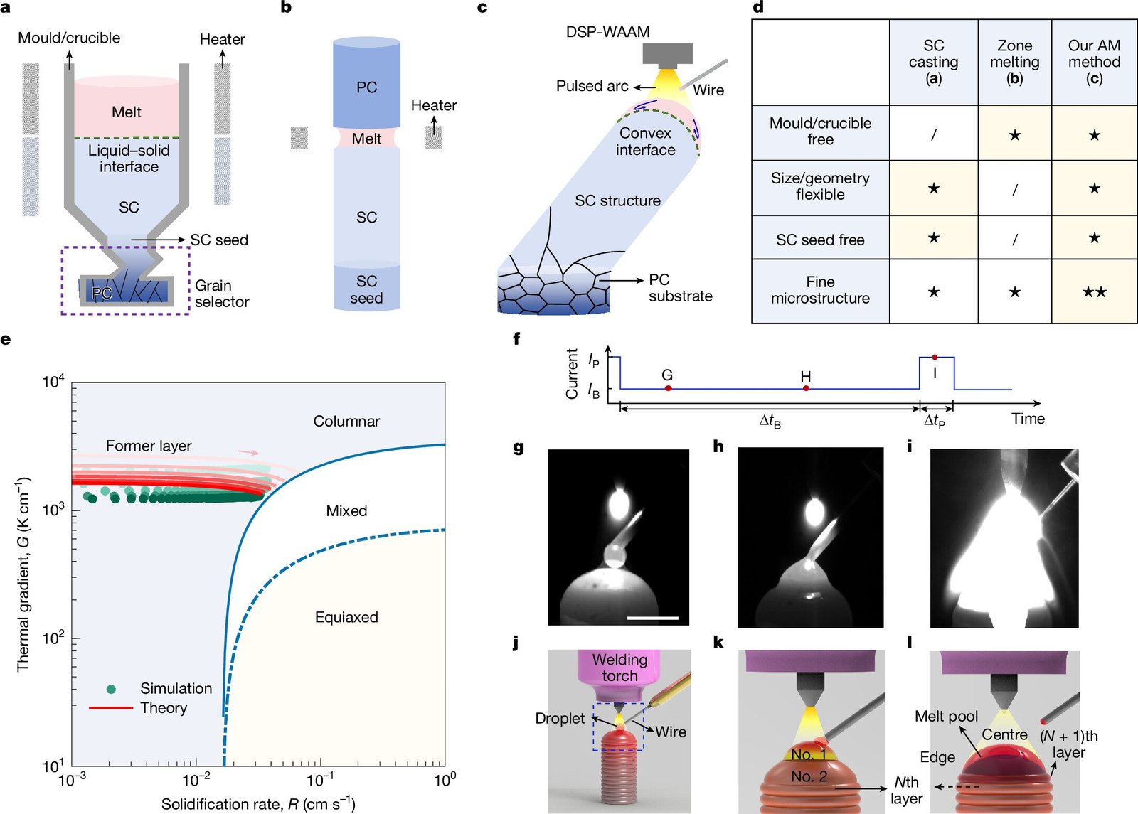
The results come from a wire-and-arc deposition technique the authors call deep-squat pulsed wire arc additive manufacturing (DSP-WAAM). Wire melts in an electric arc whose current switches between a high peak and a low base level, 200 A and 20 A in the modeled case. A section cut from the base of a niobium sample shows stray grains disappearing within a short distance as a single crystal takes over.
Thermal-fluid modeling shows why the switching is needed. Pulsing created a broad, shallow melt pool with an outward-bulging solidification front, a shape that helps eliminate unwanted grains. A steady current at the peak level overheated the deposit until it collapsed, and a steady current at the base level could not melt the wire.
Remelting provides a second safeguard, governed by a layer thickness of about 0.15 mm. The study authors write, “Notably, conventional single crystal (SC) growth relies on uninterrupted epitaxial growth but remelting in AM enhances fault tolerance: for each deposition layer, regions that deviate from this condition can be remelted, leaving the remainder as a SC. Thus, it is sufficient that only the non-remelted regions (determined by the layer thickness) satisfy the epitaxial growth condition. This enables stable SC growth in an intermittent, self-correcting, layer-by-layer manner.”
Growing Single Crystals Through Metal AM
Printing single crystals has proven difficult because crystal growth typically depends on near-steady thermal conditions, while metal AM heats and cools each layer repeatedly. Earlier efforts included small single-crystal nickel alloy deposits grown on existing single-crystal bases, as well as parts in which a single-crystal core was surrounded by polycrystalline material.
One seed-free approach came from Japan, where researchers at the National Institute for Materials Science, Kyushu University, and Osaka University 3D printed single-crystal pure nickel using selective laser melting. Laser processing of single-crystal nickel-based superalloys had usually called for a single-crystal build plate. The team instead used a flat-top laser beam to form a planar melt pool, growing single crystals on polycrystalline stainless steel plates. Like DSP-WAAM, the method shapes the melt pool to keep one crystal growing without a seed.
Seed-free single-crystal printing has now moved from pure nickel builds to titanium alloy parts a meter tall and to refractory metals such as tungsten and molybdenum.
Titled “Additive manufacturing of ultralong and architected single crystals,” the study was conducted by Changmeng Liu, Yinan Cui, Jiachen Wang, Xiao Han, Zhongao Ji, Zhun Liang, Chongle Zhang, Jaime Marian, Zixiang Li, Tao Lu, Tianqiu Xu, Jinyu Zhang, Wei Cui, Wei Liu, Daining Fang, and Y. Morris Wang.
To stay up to date with the latest 3D printing news, don’t forget to subscribe to the 3D Printing Industry newsletter or follow us on LinkedIn.
Explore the full Future of 3D Printing and Executive Survey series from 3D Printing Industry, featuring perspectives from CEOs, engineers, and industry leaders on the industrialization of additive manufacturing, 3D printing industry trends 2026, qualification, supply chains, and additive manufacturing industry analysis.
Featured image shows Principles and characteristics of the DSP-WAAM. Image via Nature.
